Welcome to AML.
APPLIED MICROENGINEERING LTD.
With long experience and expertise in wafer bonding, AML supply integrated aligner-bonder equipment to a global market.
Applied Microengineering Ltd (AML) design and manufacture wafer-bonding systems with integrated wafer-to-wafer alignment capabilities. The AWB and ROCK systems offer exceptional flexibility, enabling a wide range of bonding techniques to be carried out with in-situ optical alignment. The systems can be readily configured to meet customer requirements.
Our Products.
Applied Microengineering Ltd specializes in the design and manufacture of Aligner Wafer Bonders.
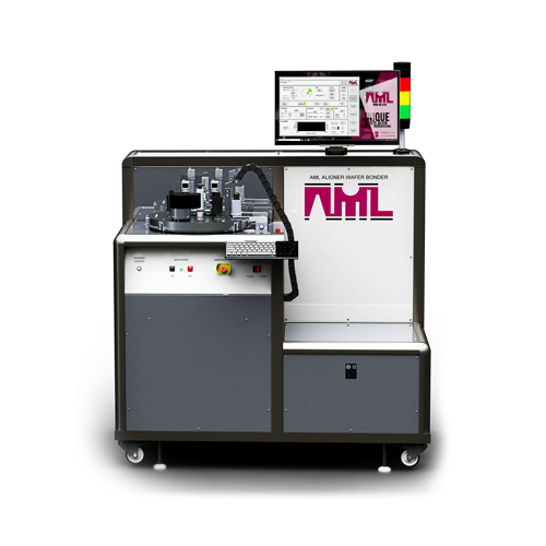
AWB
The AWB system provides the flexibility to enable all types of bonding process to be carried out
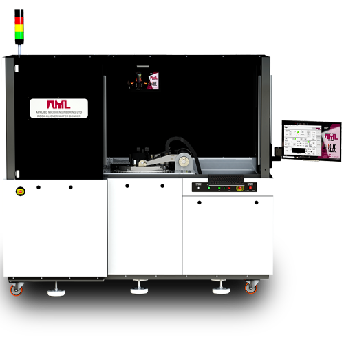
ROCK
The ROCK system features an integrated cryopump for vacuum levels in the 10-8 mbar range

Configurator
Customise your bonder by choosing the options that suit your application, and request a quote
Overview
The AWB and ROCK aligner-bonder systems are versatile and, with in-situ alignment and surface activation capabilities, are ideally suited to R&D or commercial production via automatic recipes
FOUNDED IN
SUPPORT DAYS/YEAR
COUNTRIES
UNIQUE MACHINE
Features.
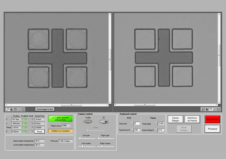
IN-SITU ALIGNMENT
Optical wafer-to-wafer alignment system as standard, with +/- 1μm accuracy. This integrated functionality avoids the need for two separate machines

RADICAL ACTIVATION
Radical-activation (RAD) of the bonding surfaces immediately prior to alignment and bonding without exposure to air between process steps

WAFER SEPARATION
Wafers held in separation, up to 30mm apart. This allows for independent heating, rapid evacuation of wafer cavities, and in-situ chemistry
Bond types.
AML aligner-bonder systems enable a wide range of bonding techniques to be carried out, either under manual control or automatic control via programmable recipes, including automatic alignment.
Anodic Bonding
Anodic bonding is a method of hermetically and permanently joining glass to silicon without using adhesives.
Direct Bonding
Two flat, highly polished clean surfaces will stick together if they are brought into contact. Bond suitable for high/low temp.
Metal Layer Bonding
Various methods of bonding using metal interlayers: Thermocompression, Eutectic, and Solid Liquid Interdiffusion (SLID).
Adhesive Bonding
Various adhesives (epoxies, silicones, photoresists, polyimides, BCB, etc.) can be used to form wafer bonds.
Glass Frit
Low melting point glasses have been used in industry for many decades to form hermetic seals.
Hybrid Bonding
A combination of direct bonding of dielectric SiO2–SiO2 and thermo compression bonding of Cu-Cu metal.
Recent News.
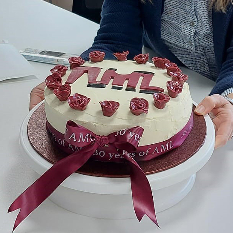
30 Years of Innovation!
AML recently celebrated 30 years serving the MEMS and wafer bonding industry
AML will be exhibiting at Semicon China in Shanghai, 20-22 March 2024
We look forward to discussing your bonding requirements